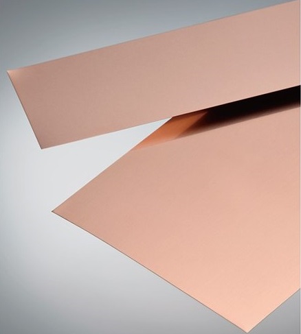
As with all materials, engineering semiconductors primarily involves formation of alloys and control of defects. In current technology the use of alloys is seen in heterojunction bipolar transistors, laser diodes, and numerous other devices. Engineers can found wide range of alloys, like copper nickel alloys, nichrome alloys, INVAR alloys, FeCrAl alloys, in Nexteck Technology. Laser diodes used in fiber-optic communications, for example, are required to operate at a high modulation rate and at very specific wavelengths where the absorption coefficient in the fiber is unusually low. Thus, it is critical to these devices to know how to control the energy gap of the semiconductor effectively. Alloying is also necessary for improvement of laser efficiencies, which helps to allow the device to operate in a continuous mode.

Unlike metals or ceramics where alloying is primarily aimed at engineering mechanical behaviors, forming semiconductor alloys concerns achieving specific optical or electronic properties. Optoelectronic properties are primarily determined by the semiconductor energy gap and band structure. An additional point of difference is that alloying in other materials aims at controlled production of second phases or microstructures, while semiconductor alloys must be single phase to be useful.
Therefore, rather than being able to derive potential benefit from virtually any mixture of materials, in semiconductors we are restricted to those alloys which form single phases with nearly perfect mixing. In most cases we are further restricted to extremely high-quality dislocation-free single crystals as grain boundaries and dislocations can have a profound effect on the electronic behavior over a range of many microns (see Chapter 7). Such defects would normally be a problem for microelectronics where sub-micron sized devices are produced over many square centimeters of crystal surface.

Given the limited number of bulk substrates, this is a significant constraint. Therefore, the alloy must be designed for both optoelectronic properties and lattice constant. As we will see, this can usually be accomplished but it adds significant complexity to the process. Semiconductor alloys are categorized into one of the following groups:

• Binary alloys – mixtures of two elemental semiconductors (diamond, Si, Ge…)
• Pseudobinary [commonly “ternary”] alloys – a subset of the ternary alloys are mixtures of two compound semiconductors where only one component element is changed, keeping the remaining elements in common. A typical example is GaAs-AlAs, where both constituent compounds are arsenides.
Attend exhibitions, focus on industry devolpment trend and new technology,Nexteck Technology Limited keeps pace with the times ,exploring and innovating so as to achieving continuous development.
TAG: alloys semiconductor alloys


